Modern computers and smartphones keep growing in capability, getting faster and more efficient with each model, and largely, that’s because the tiny microchips that power them have been evolving at an unprecedented rate. As Moore’s Law predicts, the number of transistors that an electronics-powering chip can hold is supposed to more or less double every two years. More transistors means speedier chips capable of performing more calculations, but achieving that without changing the size of the chips has computer engineers worried about running out of space.
“Historically, transistors have been built to lie flat upon the surface of a semiconductor, with the electric current flowing laterally, or side-to-side, through them,” IBM said in a press release this week about a new chip architecture design that they’re also presenting tomorrow at the 2021 International Electron Devices meeting. “With new Vertical Transport Field Effect Transistors, or VTFET, IBM and Samsung have successfully implemented transistors that are built perpendicular to the surface of the chip with a vertical, or up-and-down, current flow.”
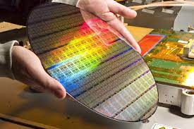
To understand why this is potentially a big deal for semiconductor technology, it makes sense to first focus on individual transistors for a moment. “The DNA of any hardware technology is the transistor,” says Hemanth Jagannathan, a researcher at IBM. Billions of transistors can cover the surface of a silicon wafer, and these wafers are layered together to make a microchip.
A typical, standard transistor that’s commonly found in electronics has three terminals: source, gate, drain. The current (which is a stream of electrons) flows from source to drain. The gates control the flow of currents and dictate the state of the transistor. When voltage is applied to the gate, the transistor is turned on and in state 1. When no current is flowing between the source and drain, the state is 0. Additionally, two separate transistors need a region in between to isolate them and prevent them from interfering with one another, and this is done with dummy gates.
Then there is a concept called “contacted gate pitch” which is the physical distance required to fit all the transistor components. “These are very basic structural requirements, and you can think of two hard walls and you have to fit the gate, the spacer, and the region for contact within that,” says Jagannathan. The walls keep closing in, but at some point, they can’t come any closer without sacrificing functionality.
Previous transistor innovations like FinFETs and nanosheets, have the gate, source, and drain on the same plane. With a vertical design, these structures essentially get stacked on top of each other, on the wafer. Plus, vertical transistors don’t need a dummy gate—they instead use something called shallow trench isolation, which conserves space.
Source : https://www.popsci.com/technology/ibm-samsung-vertical-transistors-semiconductor-technology/